Updated my TTGO v2.1 1.6 enclosure design. TTN logo is now up straight + all buttons and connectors exposed (including led lights).
1 Like
Hi, I recently bought a pair of TTGO32V20 and a TTGO-Beam. Am able to get direct-lora connections to work through the Arduino programming environment. Nice.
Am unable to get the TTGO32V20 working on TTN. Although I read all 3 topics (and a lot more) I guess I missed something.
My baseline is the coding by NicBKW (BIG ESP32 / SX127x topic part 1)
I wired D1 to pin 33
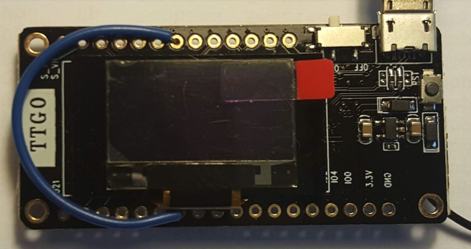
I made pin mapping as follows:
// Pin mapping
const lmic_pinmap lmic_pins = {
.nss = 18,
.rxtx = LMIC_UNUSED_PIN,
.rst = LMIC_UNUSED_PIN,
.dio = {26, 33, LMIC_UNUSED_PIN},
};
My TTN settings are as follow:
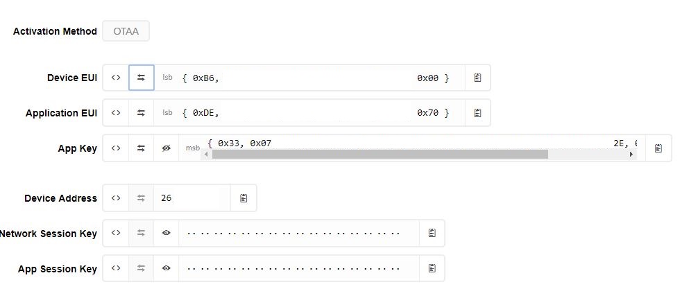
Added DEVICE EUI and APPLICATION EUI as little endian (LSB first).
Coding:
static const u1_t PROGMEM APPEUI[8] = { 0xDE, … 0x70 };
static const u1_t PROGMEM DEVEUI[8] ={ 0xB6, … 0x00 };
static const u1_t PROGMEM APPKEY[16] = { 0x33, … 0x3A, 0x35 };
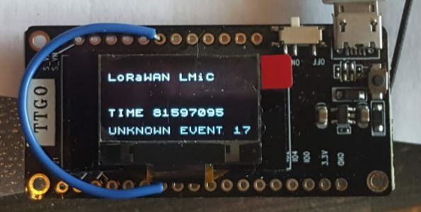
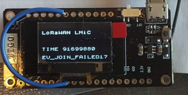
And it does not work. I believe error 17 “something else”.
I compiled PAXCounter from PlatformIO (unknown to PlatformIO, but I eventually managed to upload) and after some time I saw the green button “last seen …few minutes ago”. No payload though, but I am not interested in getting PAXcounter to work, just checking if there is a hardware failure. So there is not.
What am I missing?
[update]
Two screen shots, Unknown Event17 and Join Failed 17.
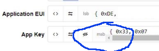
In your above screenshot, the AppKey is displayed in msb. Can you double check that?
The AppKey may probably be the issue here, but my advice is to always start with ABP (ttn-abp.ino) first as this will rule out any possible OTAA issues. If ABP works you know that at least the node (hardware and LMIC) is working.
2 Likes
In the picture you can see it reads LSB, so…
Where can I find the ttn-abp.ino?
Further more… thee are several LMIC libraries out there and I am confused which one to use.
No need to be confused, read the Topic Start.
(If you would need any other version then you will have a specific reason for that.)
Read the Topic Start.
1 Like
In the picture you can see it reads LSB, so…
I am confused, in your screenshot I am reading MSB, that’s why I said it was worth double checking
Using a Heltec LoRa32 V2 with PIN configuration as stated in
https://www.thethingsnetwork.org/forum/t/big-esp32-sx127x-topic-part-2/11973/843
the device appears to be sending properly, but TTN never receives anything. With a V1 Heltec device, everything is fine. Does someone have any working code for Heltec LoRa32 V2?
1 Like
Read the TOPIC START
The correct configuration parameters are specified in the Topic Start (and they normally work).
If you find any possible issues or missing information in the Topic Start then please share so I can fix it and update the topic start.
Update:
And for me: better read the new V2 pinout diagram. 
Well, they don’t work for the V2 version of the Heltec device, at least not for mine. Do I have to assume that mine is broken?
@saglettn Is your V2 board some new version (see below)?
I have some questions about (new) Heltec Wifi LoRa 32 ‘V2’ boards:
-
Has a new Heltec Wifi LoRa 32 V2 been recently released that is different from the existing ‘V2’?
(Heltec initially was not using V1 and V2 in the names or on the PCB, which is why I introduced version numbers V1 and V2 for existing Heltec boards earlier this year. Now in the V2 pinout diagram I do see V2 marked on top of the PCB.) -
Is your V2 PCB explicitly marked with a version number?
Is it like the version number shown in the V2 pinout diagram? -
Are there any known differences?
In this post:
@saglettn mentions a ‘new’ pinout for the Heltec V2.
On the pinout I see “V2” marked on the PCB but I see no pinout differences when comparing it to the previous Heltec Wifi LoRa 32 pinout diagram (the one mentioned in the Topic Start). Only the board picture seems to have been updated. DIO0, DIO1 and DIO2 are still not listed in the new pinout so it’s impossible to see if their pinouts/connections have been changed (DIO0 is still called LoRa_IRQ in the V2 diagram). The V2 diagram also contains a sloppy error: the legenda has been moved to the right but ‘Button’ and ‘Touch1’ which belong to GPIO0 have also been moved - incorrectly. So how reliable is the V2 diagram?
In this post:
@Verkehrsrot states DIO1 = 34 and DIO2 = 35.
@saglettn confirms this works. The values for Heltec ‘V1’ and ‘V2’ have been DIO1 = 33 and DIO2 = 32.
Has Heltec changed this on a new version of their boards?
YES, see further below.
Thanks for getting into those details.
I have a V1 Heltec device, which works perfectly fine with the .dio = {/dio0/ 26, /dio1/ 33, /dio2/ 32} setting from topic start.
My V2 Heltec device has printed “V2” on the PCB, where “WiFi LoRa 32” was printed on the V1, i.e., on the top side where the OLED is. I think they’re manufacturing it since August 2018.
With this V2 Heltec device,
-
when I use my original working code from the V1 device, it just hangs on scheduling the packet and never sends it. Thus I assume that something must have changed on the hardware side.
-
when I use the .dio 34, 35 setting posted by @Verkehrsrot, it looks like the packet is sent, even a TX_COMPLETE event is triggered, but it doesn’t get trough to the gateway and TTN (I have my own multi-channel gateway 10m away and it works perfectly fine with my other devices, and use the external antenna that is shipped by Heltec, so I’m confident it’s not a range issue).
Am I maybe missing some wiring/soldering required that was not necessary with the V1 Heltec device?
I have a one year old Heltec Wifi LoRa 32 ‘V2’ as pictured in the topic start.
That one runs fine with the configuration parameter values described in the topic start.
So, apparently Heltec has made some changes (or there is an issue with your board).
Are you using OTAA?
Are you using one of the standard examples (ttn-otaa.ino, ttn-abp.ino) or a custom sketch?
when I use my original working code from the V1 device, it just hangs on scheduling the packet and never sends it.
That sounds like a DIO (mis)configuration issue.
when I use the .dio 34, 35 setting posted by @Verkehrsrot, it looks like the packet is sent, even a TX_COMPLETE event is triggered, but it doesn’t get trough to the gateway and TTN (I have my own multi-channel gateway 10m away and it works perfectly fine with my other devices,
When using the ttn-otaa.ino example the TX_COMPLETE normally only fires when the OTAA join was successful. OTAA join can only be successful if the connection to the gateway and the TTN backend work successfully.
Best to start with ABP / ttn-abp.ino to rule out possible OTAA issues.
Are you sure everything on the node and backend is configured correctly?
Am I maybe missing some wiring/soldering required that was not necessary with the V1 Heltec device?
Soldering was not required for V1 and the ‘old V2’ (without the V2 marking on the PCB).
Whether manually connecting/soldering DIO ports (board pins or solder pads) to GPIO ports (board pins) is required depends on possible changes. You would need to find out if and which LoRa DIO’s are actually connected to GPIO ports of the ESP32. This could be done with a multimeter with very fine measuring tips.
But if that would be necessary (like with TTGO V2+ boards) then the board would need to have board pins that are only used for DIO ports, or solder pads on the PCB (usually clearly marked). From the V2 diagram this appears not to be the case. But my experience with these diagrams is that they are often not reliable an not (frequently) updated.
FYI, LMIC use of DIO ports: ABP uses/requires DIO0, OTAA requires both DIO0 and DIO1. DIO2 is not used for LoRa.
The V2 I have is presented with a picture under http://www.heltec.cn/project/wifi-lora-32/?lang=en . You can see the “V2” printed on the PCB next to the antenna connector there.
I use ABP, and have 6 other nodes in the same TTN app, which all work fine. So I’m never sure that everything is configured properly, but I am pretty confident.  Seriously, this V2 Heltec is the only LoRa device I have that ever gave me serious trouble.
I’ll check the DIO / GPIO port connections.
According to Heltec’s pinout documentation:
DIO0: GPIO 34
DIO1: GPIO 35
Heltec’s pinout file is called WIFI LoRa 32(V2) .pdf. The documentation at the top of this topic links to a different pinout. In this topic it’s listed for a Heltec Wifi LoRa 32 V2 board. But it seems to be the same picture as the one that Heltec calls WIFI LoRa 32 .pdf (see here). Do more than two versions of this board exist? Or is the above link incorrect?
I totally overlooked the DIO0: GPIO 34 and DIO1: GPIO 35 in the new V2 pinout diagram.
The new V2 pinout diagram is still not correct however. DIO0 appears still listed as “LoRa_IRQ” and probably “DIO0” should be DIO1 and “DIO1” should be DIO2. Another possibility is that the labels “DIO0” and “DIO1” are correct and the “LoRa_IRQ” label is a leftover that was forgotten to be removed from the diagram. I don’t have the hardware to verify these assumptions however.
The new board which Heltec now calls V2 is actually V3.
The first ‘V1’ board is shown in the Topic Start and so is ‘V2’.
These version numbers were introduced by me, not by Heltec (as already mentioned in the Topic Start).
While Heltec had different board before, they were not using version numbers.
The impression I get is what I called V1 is only available for 433MHz and what I called V2 is only available for 868/915MHz and Heltec (now) calls both these boards ‘V1’: V1 433MHz and V1 868MHz. Even while they are different versions, not just their LoRa frequencies but also the implementation of the Wifi antenna and PCB.
To prevent future confusion the naming and version numbers used in the Topic Start need to be updated (soon) to reflect Heltec’s current names and version numbers.
I hope this clears things up.
Hi, to sum up:
Heltec Wifi LoRa 32
Have a white PCB and come in two different versions (the version numbers are not used by Heltec) :
- V1-433MHz : with on-board PCB WiFi/Bluetooth antenna. Appears to be available for 433MHz only.
-
V1-868/915MHz : with small on-board helical antenna (has a PCB antenna on the bottom but that is not connected) .
Heltec Wifi LoRa 32 pinout diagram . -
V2-868/915MHz : with small on-board helical antenna (has a PCB antenna on the bottom but that is not connected) AND V2 writen close to LoRa antenna connector
Heltec Wifi LoRa 32 V2 pinout diagram
TTGO T-BEAM with GPS onboard (without display)
This is the new board with GPS included
T-beam pinout
TTGO LoRa and TTGO LoRa32
Have a black PCB and come in several different versions:
- LoRa with on-board PCB Wifi/Bluetooth antenna on top. Appears to be available for 433MHz only(?). Also available without the display.
- LoRa32 V1 : with on-board metal Wifi/Bluetooth antenna on bottom. I-Pex connector located on top.
-
LoRa32 V2 : with on-board metal Wifi/Bluetooth antenna on bottom (in a different location).
Uses ESP32-Pico-D4 (with integrated flash memory) instead of ESP32, uses a (shielded) LoRa module, I-Pex connector located on the bottom, micro-USB connector is rotated 90 degrees, in addition has a microSD card slot on the bottom and an on/off switch for the battery next to the micro-USB connector. Switches the battery only so not possible to switch the board off when connected to USB for charging the battery.
‘Programmable’ LED on pin 22 instead of pin 25 but useless because wired to SCL and all three LEDs are on the bottom side where you cannot see them. DIO1 and DIO2 each have a separate board pin but neither of them is connected to a GPIO port so must be explicitly wired. This also means that the TTGO V2 has two GPIO ports less that could otherwise have been used for other purposes.
The microSD card slot can be used as a regular SD card reader/writer. The LoRa modules are HPD13A and HPD14A from HPDTek.
New updated pinout diagram v3.0 is available here: TTGO LoRa32 V2.0 Pinout v3.0.pdf (2.3 MB) -
LoRa32 V2.1 : Like V2.0 with several changes and improvements (e.g. SMA LoRa antenna connector, different battery charging chip, different switch). Some changes in use of pins / GPIO’s. Different versions of this board exist (some differences in GPIO/pin mappings between versions).
TTGO LoRa32 V2.1 pinout diagram possibly not up to date. Do not use this pinout for LoRa32 V2.1 with PCB marked V1.6 because it is incompatible.
How to configure LMIC with the ESP32 pins used for the LoRa module:
//LMIC LoRa module pin configuration

//For Heltec Wifi LoRa 32 V1, TTGO LoRa and TTGO LoRa32 V1 use:
const lmic_pinmap lmic_pins = {
    .nss = 18,
    .rxtx = LMIC_UNUSED_PIN,
    .rst = 14,
    .dio = {/*dio0*/ 26, /*dio1*/ 33, /*dio2*/ 32}
};
//For Heltec Wifi LoRa 32 V2, TTGO LoRa and TTGO LoRa32 V1 use:
const lmic_pinmap lmic_pins = {
    .nss = 18,
    .rxtx = LMIC_UNUSED_PIN,
    .rst = 14,
    .dio = {/*dio0*/ 26, /*dio1*/ 34, /*dio2*/ 35}
};
//For TTGO LoRa32 V2 use:
//Note: LoRa32 V2 DIO1 and DIO2 are not on-board wired to any GPIO.
//These need to be wired manually.
//DIO2 is actually not needed for LoRa(WAN) so does not need to be wired.

const lmic_pinmap lmic_pins = {
    .nss = 18,
    .rxtx = LMIC_UNUSED_PIN,
    .rst = LMIC_UNUSED_PIN,
    //If DIO2 is not connected use:
    .dio = {/*dio0*/ 26, /*dio1*/ 33, /*dio2*/ LMIC_UNUSED_PIN}
    //If DIO2 is connected use:
    //.dio = {/*dio0*/ 26, /*dio1*/ 33, /*dio2*/ 32}
}
//For TTGO LoRa32 V2.1:
//The first revision(s) does not have LoRa RST connected to GPIO, use as V2 above.
//(DIO2 is actually not needed for LoRa(WAN) so does not need to be wired.)
//Revision V1.5 (V1.5 marked on PCB) uses GPIO12 for LoRa RST.
//Revision(s) newer than V1.5 use GPIO19 for LoRa RST.
//Note: On first revision(s) DIO1 and DIO2 are not on-board wired to any GPIO and have to be wired manually.
//Later revisions may have these wired on-board already.

const lmic_pinmap lmic_pins = {
    .nss = 18,
    .rxtx = LMIC_UNUSED_PIN,

    //For board revision V1.5 use GPIO12 for LoRa RST
    .rst = 12,
    //For board revision(s) newer than V1.5 use GPIO19 for LoRa RST
    //.rst = 19,

    //If DIO2 is not connected use:
    .dio = {/*dio0*/ 26, /*dio1*/ 33, /*dio2*/ LMIC_UNUSED_PIN}
    //If DIO2 is connected use:
    //.dio = {/*dio0*/ 26, /*dio1*/ 33, /*dio2*/ 32}
}
//For TTGO TBEAM:
// Pin mapping
const lmic_pinmap lmic_pins = {
  .nss = 18,
  .rxtx = LMIC_UNUSED_PIN,
  .rst = LMIC_UNUSED_PIN, // was "14,"
  .dio = {26, 33, 32},
};
2 Likes
Thanks for the summary. 
I will update the topic start with what’s changed or added/new (soon).
So, paxcounter settings for heltec v2 aka “V3” found here should be correct:
For the TTGO TBEAM version T22_V07 (20180711)
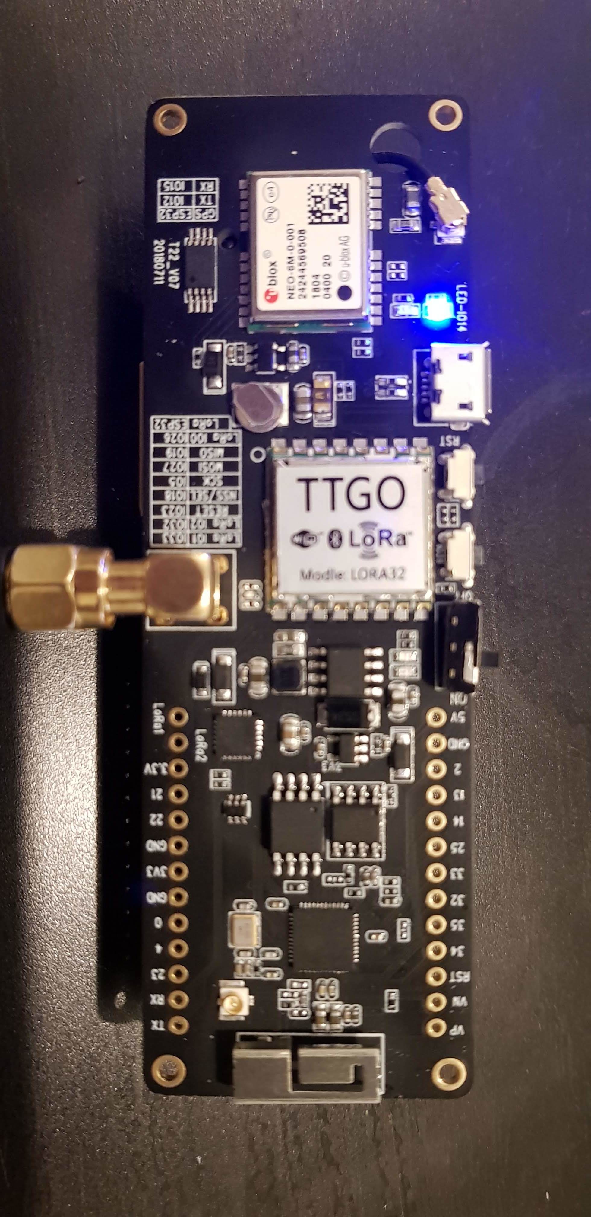
Here is an extract of the file ttgobeam.h for the paxcounter application:
#define HAS_LED GPIO_NUM_14 // on board green LED
// Pins for LORA chip SPI interface, reset line and interrupt lines
#define LORA_SCK (5)
#define LORA_CS (18)
#define LORA_MISO (19)
#define LORA_MOSI (27)
#define LORA_RST (23)
#define LORA_IO0 (26)
#define LORA_IO1 (33)
#define LORA_IO2 (32)
And the platformio.ini file:
[platformio]
env_default = ttgobeam