Today I published a “Nano power system” for powering LoRa endnodes. During idle time, the power consumption is well below 1 micro ampere. You can find documentation of this project here.
1 Like
tnx 
I converted your file to Low power system.pdf (326.0 KB)
* uncheck framecounter checks as advised is off course not very safe and should be used only for testing
I know about the framecounters. In most cases using flash is a good option.
That’s interesting, I’m using the same chip for some time, but with less components, the node says to the TPL it’s finished with the done pin, couldn’t be simplest 
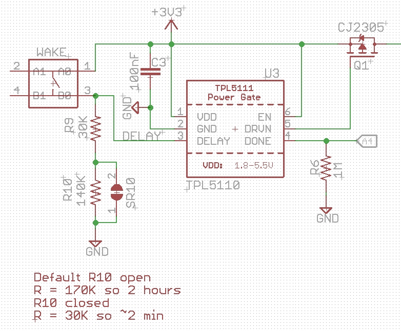
I also use it with another option, wake from deep sleep (no BOD, no watchdog, …) with the DRVN pin connected to a I/O that wake up the node with interrupt (in this case node does not reboot, just wake), the mosfet in this case is used to poweroff all other hardware (sensors, RF module, Flash, …)
1 Like
Very interesting. I wonder if some sort of programmable resistor could be used so that the MCU chooses for how long the next sleep will last.
Hard to do, as the resistor is only measured on power-up.
Nice job. I do have some suggested improvements / observations
- The schematic has two C1s on it but only one capacitor on the prototype
- It is exceedingly unlikely that power consumption will be below 1uA in idle because of the use of Electrolytic capacitors, The leakage of these alone will exceed 1uA. Try using ceramic capacitors instead.
- The use of the startup delay extension is intended to deal with the startup time of the processors however modern processors will achieve oscillator lock in the order of a few microseconds and, where power up timers are implemented, the startup time is in the low milliseconds. The reasons that a processor can take longer to start up are due to either external factors, such as a Capacitor on the reset pin which would not be required with this schematic of because the application software includes a bootloader that is waiting to be capture. In the event of a bootloader being the culprit you can address this by having the bootloader assert the hold pin immediately it starts executing or get rid of the bootloader.
- The current consumption during the non idle time (2.x seconds) could be improved which would improve the overall efficiency. Examples include Increasing R6 to 1M, inserting a 10K or higher resistor between the collector of T1 and the base of T2 leaving R4 on the collector of T1. This resistor limits the wasted base current into T2 which can be between 3mA and 30mA depending on the hfe of T1. Increase R4 and R5 to 220K.
Then, on a more trivial note, T1 and T2 instead of being general purpose transistors could be replaced with FETs which would remove the base-emitter current inefficiency.
1- The lower C1 was an old design. I will remove it in the drawing.
2- C1 has no charge in idle mode, so no leakage. Using low leakage capacitor is always a good idea though.
3 - It takes one second to start an STM32F103, no bootloader. Maybe this has to do with capacitors on the board indeed.
4- There’s definitively something wrong there. It was not intended to have a high base current into T3. I will sort this out.