Hello to everyone!
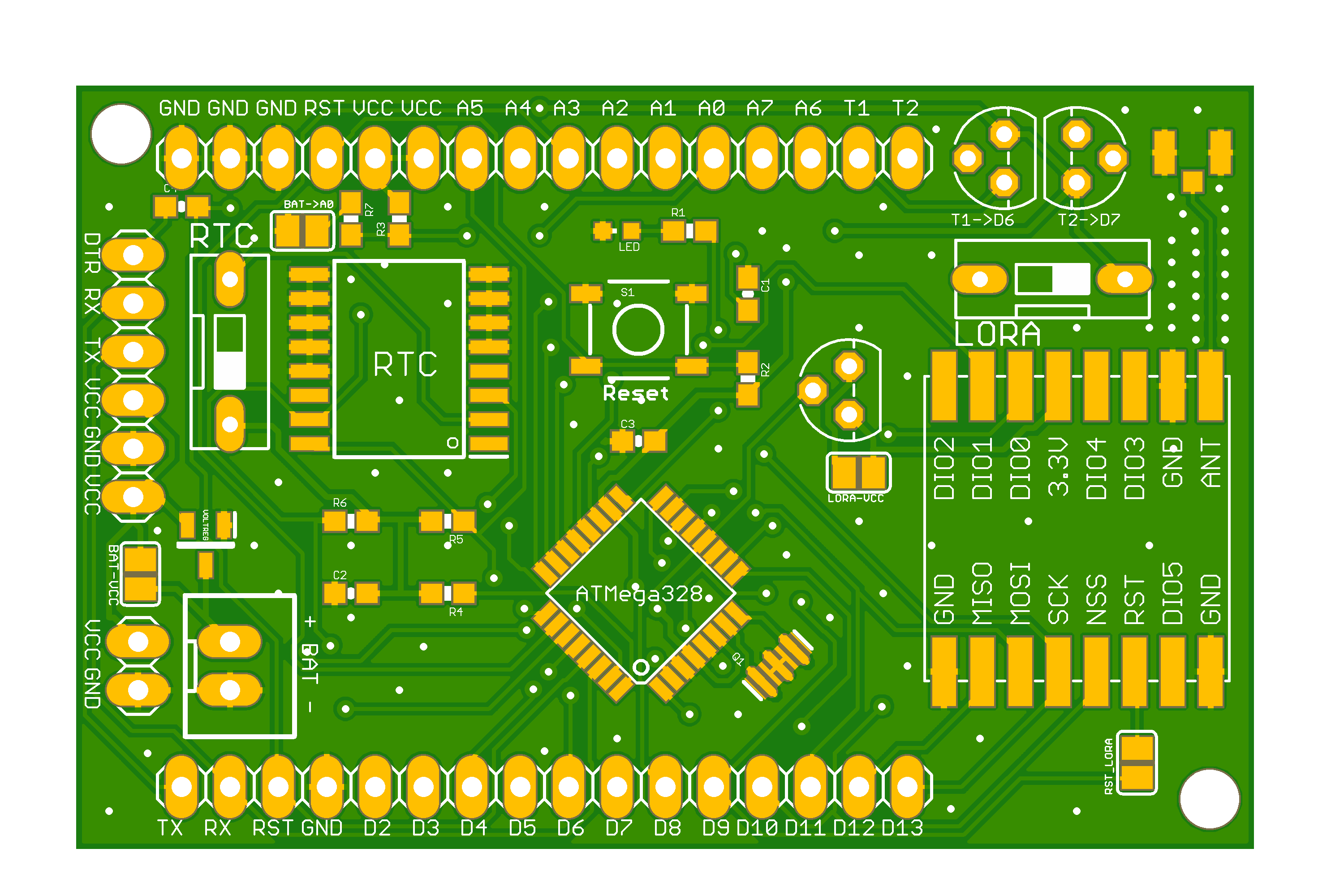
I’m developing LoRa node board which I named Butterfly.
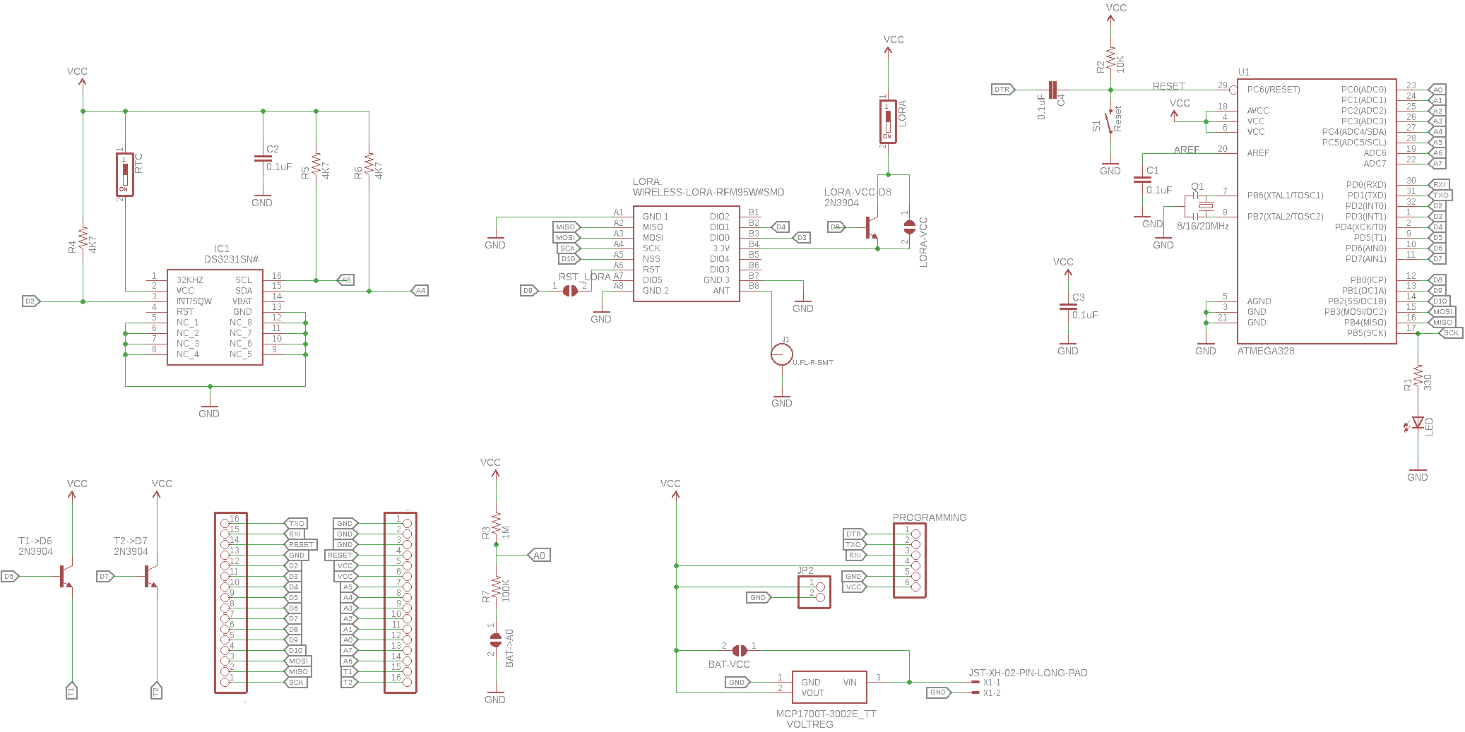
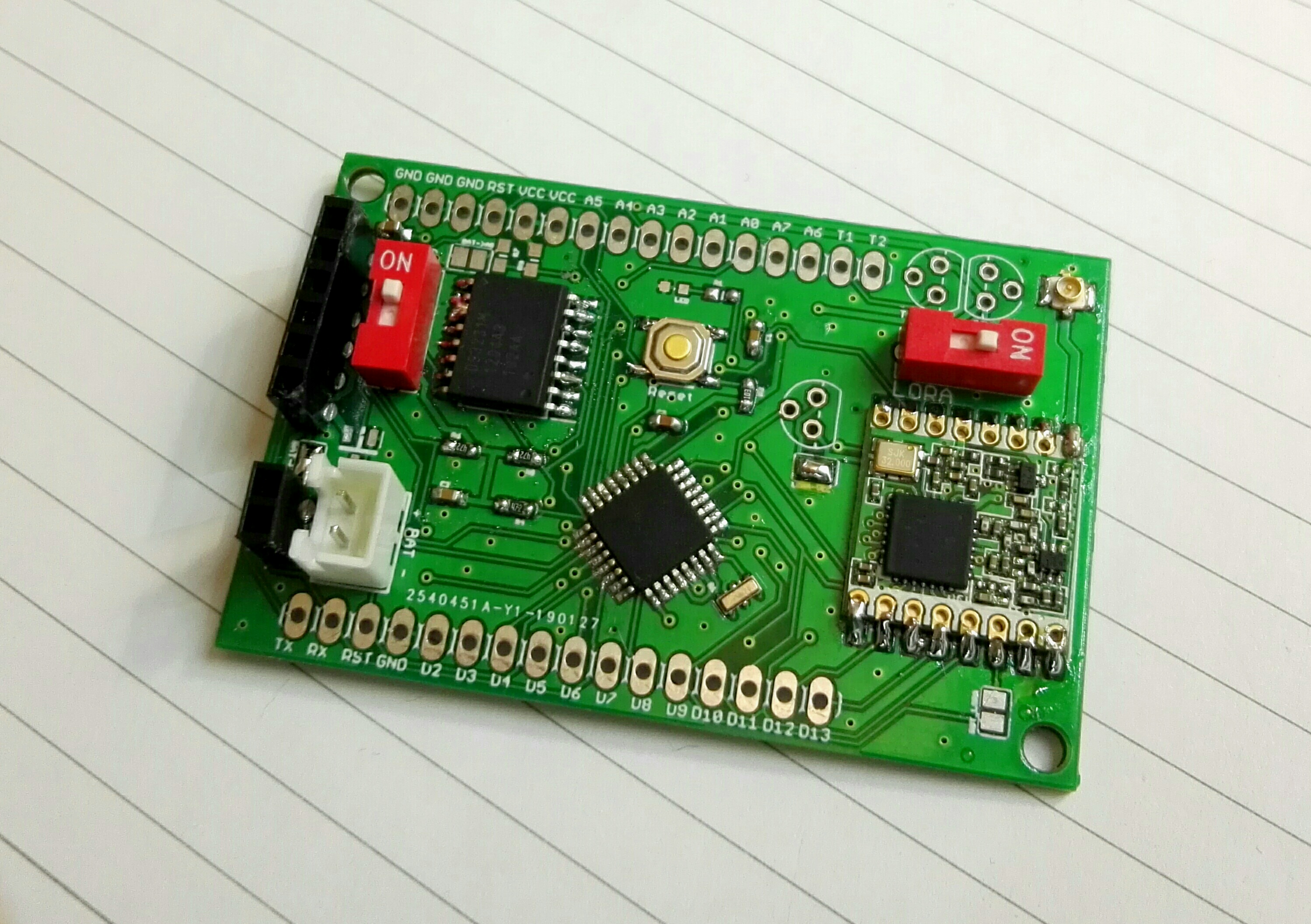
It is based on ATMega328 microprocessor (same as Arduino Mini Pro) and have RTC on itself. Idea is to have board that is great for low power testing, and great for debugging. Because of that, there would be power switches for LoRa module and RTC (DS3231 chip) so you can turn it on/off when you want. If you don’t need none of that you can turn of both and use this board as you used Arduino Mini Pro.
Also, there is transistor as switch if you want to regulate work of LoRa module (RFM95W) with it. When you give signal from digital pin, it will turn on or off. If you don’t want use transistor, I left jumper in parallel so you can connect it directly to VCC.
There are two more transistors if you want to control powering of some power-hungry sensor because it is recommended at ATMega328 to not pull more than 50mA from digital pin. Some sensors take more than 100mA (air quality sensor, soil moisture, GPS).
RTC is based on DS3231 chip and can be used for setting alarm for wakeup time of board. It is connected to D2 pin so you can interupt microprocessor. It is great if you want change wake up intervals from distance. It is possible with downlink messages from TTN server.
There is no LEDs except one signal LED.
I left 2 input pins for powering board (VCC pins). One is recommended to use with up to 3.7V (D size battery for example). And other is XH battery pin which can be connected to MCP1700-300 voltage regulator (if you use LiPo batteries which are on 4.2V when fully charged). If you won’t use voltage bigger than 3.7V, you can take out voltage regulator and connect that XH battery pin with jumper directly to VCC pin.
Everything will be programmed with USB programmator.
Size of board is 62mm*40mm (size of D size battery or 26650 size battery).
This is Butterfly v2.0 board. I already tested this features on v1.0 and everything worked, but now I made some improvements and waiting for new board to test it.
Power consumption goes down to 10uA with LowPower library.
Here you can see board design. All comments are wellcome!
And if you have any suggestions or advices, I will be happy to hear.
And stay tuned…
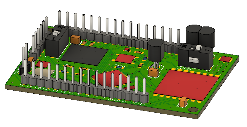
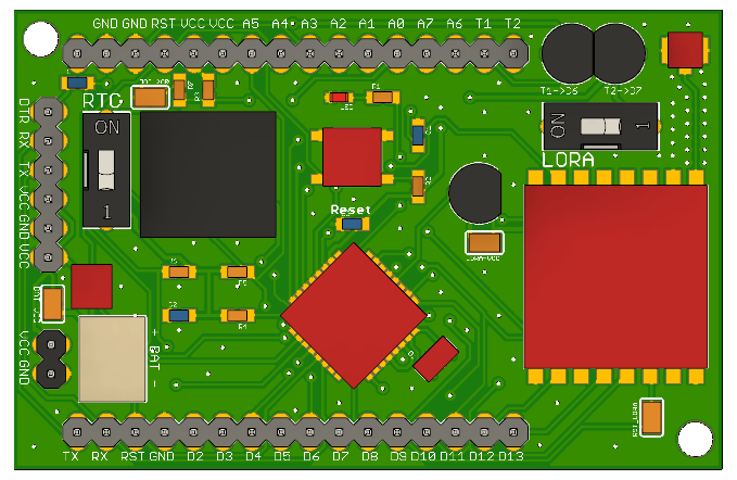
I made some kind of 3D preview but didn’t have time to find 3D model of every component.
Indeed, very difficult to comment on a PCB layout without a schematic.
Its really hard to tell, but I cannot see a pullup resistor on the LoRa device NSS, without it you will have problems programming the ATmega with an ISP programmer.
Whilst the sleep current of 10uA is not an issue in itself since even at that level the impact on a real world projects battery life is not at all significant; an ATmega setup using a DS3231 as a wakeup controller ought to have a sleep current of around 2uA without a regulator, 3uA with a regulator.
With 2 layer PCB, that RF track is too thin. Unless it’s a 4 layer board, I’m sure that needs to be thicker. Also if you take a look at the uFL connector datasheet by Hirose, the inner top layer between the pads shouldn’t have copper.
Far better in my opinion to have the pads to allow an SMA edge connector, there looks like space. If you get the tracks right you can put the pads for the u.fl in the same location, then you have the choice of a slightly dubious RF connector or a decent SMA one that you can fit an antenna direct to.
@LoRaTracker I didn’t use pullup resistor and I didn’t have problems with programming at all.
Yes, based on ATmega and DS3231 datasheets it go down to 1uA in sleep state, but I didn’t tested it yet. But when you take calculation, as you said, sleep current is not an issue. Even if it is 10uA, it means that it take 0,24mAh per days which is not big problem. But soon I will test it and see what is real consumption.
I put uFL because with one connector you can use it close to board, or even further. I think that is in most cases restrictive to use SMA on board because of using enclosure. But I will think about putting it on board. Thanks for advice.
@rocketscream This is 2 layer board. Thank you for advices! I’m new in board designs and learn every day. I will fix that.
When you connect an ISP programmer, the NSS to the LoRa device will be floating, meaning it can be selected, and thus MISO on the LoRa device goes active, directly interferring with the ISP programmer. I have always needed the pull up on my boards, if I want to use the ISP programmer.
Oh, and before you get the PCB you absolutly do need to test the circuit on a breadboard very odd things can happen to sleep current and some components might not work as expected, for instance I doubt the way you have the DS3231 connected it will work as intended …