In addition to turning off/down the BOD, you could try reducing the transmit power on the radio to see if that makes a difference. Firmware bugs can also cause a sudden reset.
I don’t recommend soldering random capacitors to the end of the antenna.
At the frequencies involved one must also consider the inductance of the leads of your capacitor, and the PCB traces. It would take fairly expensive RF geometric modeling software to figure out exactly what you’ve done, but it is a thoroughly bad idea.
Your success at this point is pretty much pure coincidence - you have an actual issue (perhaps with a noisy power supply) and you do not currently know what it is.
Did you try my suggested modifications to your code?
The default state of I/O is input mode. The standard input protection circuitry on an input has an effective diode pull-up to VCC. RF input on an unterminated input is passed by the input protection diode to the VCC. High values of RF and/or insufficient bypass on the inputs and power supply decoupling will cause all sorts of problems. This is why I suggested setting all unused pins to outputs.
I tried to say so at the beginning. But because it is so far the only working solution, I am using what I have… With my next board I can try the things that @Sandgroper proposed.
No, that would make it unusable. The VCC clamp diode is a pull down for out of range pin voltage, it’s the GND clamp diode that could be viewed as a pull up.
Probably not. Go ahead and calculate the voltage needed to forward bias the diode compared to the available RF power levels. Then calculate the amount of power able to be delivered into the supply rail.
If this were a broadcast transmitter you might have a point…
I am not wrong. Page 58 of the Atmega328p datasheet (http://ww1.microchip.com/downloads/en/DeviceDoc/Atmel-7810-Automotive-Microcontrollers-ATmega328P_Datasheet.pdf) shows the I/O Pin Equivalent circuit for this processor clearly showing the protection diode to the power rail. This is why you also see cheap level converters from 12 volt to +5v of the processor using a simple series resistor as opposed to a traditional level converter with the series resistor limiting the input current.
No, you are wrong. There is a diode of course, but as I explained, the direction is opposite of what you claimed.
You erroneously claimed “The standard input protection circuitry on an input has an effective diode pull-up to VCC.”
Because a diode would be a very “stiff” pullup, having a diode in that direction would make the pin essentially unusable - you wouldn’t be able to internally or externally drive the pin more than a diode drop below VCC without overstressing and cooking the diode.
In actual fact the IO clamp diode is oriented the other way, it is a “pull down” preventing the voltage on the pin from exceeding VCC by more than a diode drop.
The other diode prevents the voltage from dropping more than a diode drop below ground.
So two things happen with the input protection diodes. The input protection diode to VDD will result in the VDD increasing. You see this effect when you power off the processor by removing the power to the regulator and yet the processor can still run because it is being powered via voltages being present on the input pins. How much it raises VDD depends on many factors but it is easy to test.
The pull down diode (from input to ground) has the opposite effect, a negative signal below the ground rail, will drive the ground rail lower.
If the power supply impedance to the processor power pins is not low enough the power rails will effective be modulated by the RF signal. There is nothing clean about this.
As I pointed out several posts ago, that would only be true if the diode actually becomes forward biased. Given the absolute maximum ratings are half a volt outside the rails, that’s going to require something like 500-600 mV amplitude at the receiving side of the coupling - or several volts if the pin wasn’t already DC biased to the rail.
For a DC source like an externally driven I/O, sure, but you are proposing coupled RF, which is unlikely to be coupling enough energy to raise the rail much at all.
If this were a high power transmitter, you might have a point. But at the power levels actually supported, it’s a bit unlikely.
If the supply biasing doesn’t create a low impedance at RF, then your digital circuitry is itself a radio jammer splattering harmonics of clock fractions all over the place.
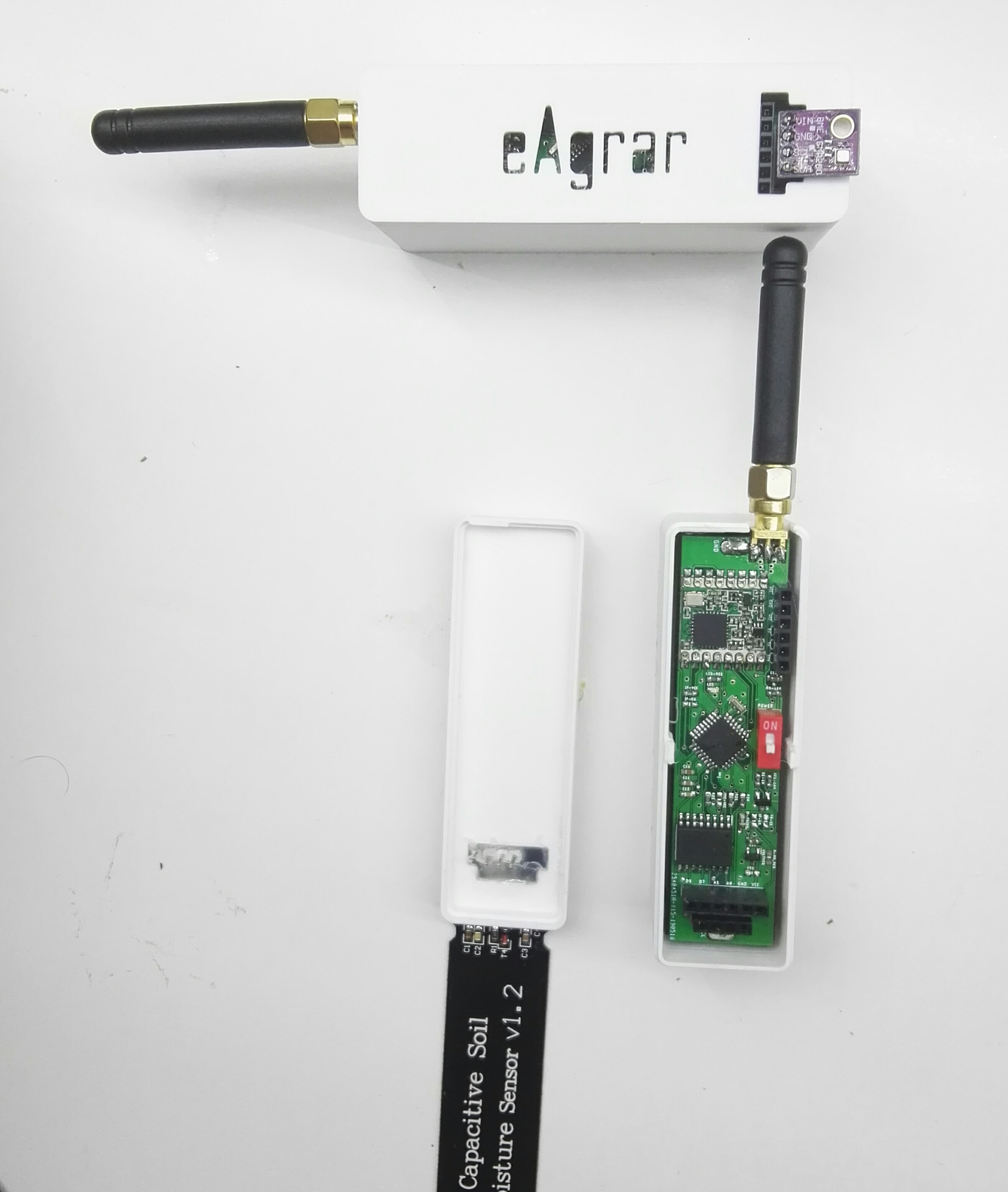
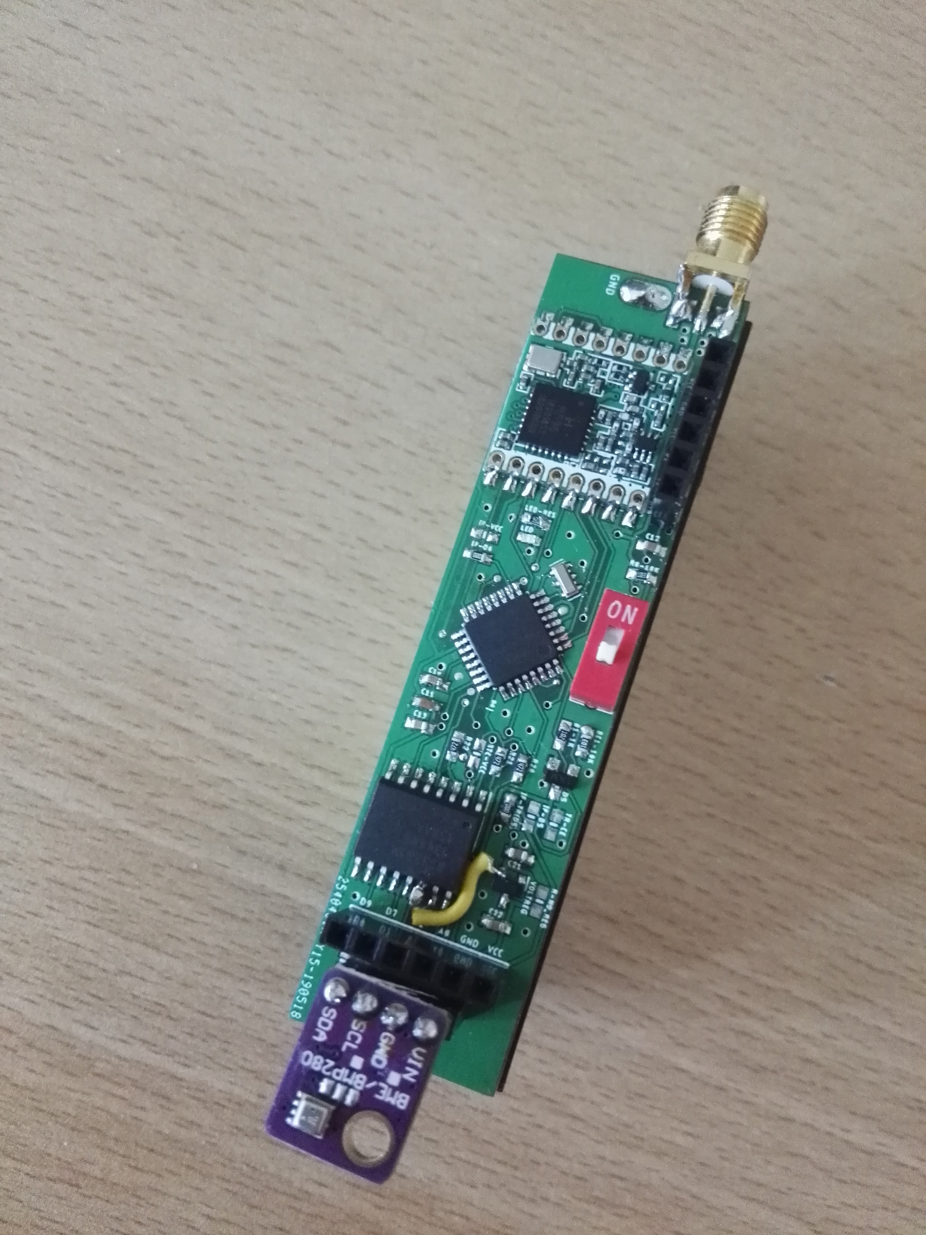
I have same problem on my board. I developed my board, and one board sometimes go to reboot loop. I found out that this happens when there is no antena attached to this SMA connector, or antenna is small and bad. Try to solder another antenna.