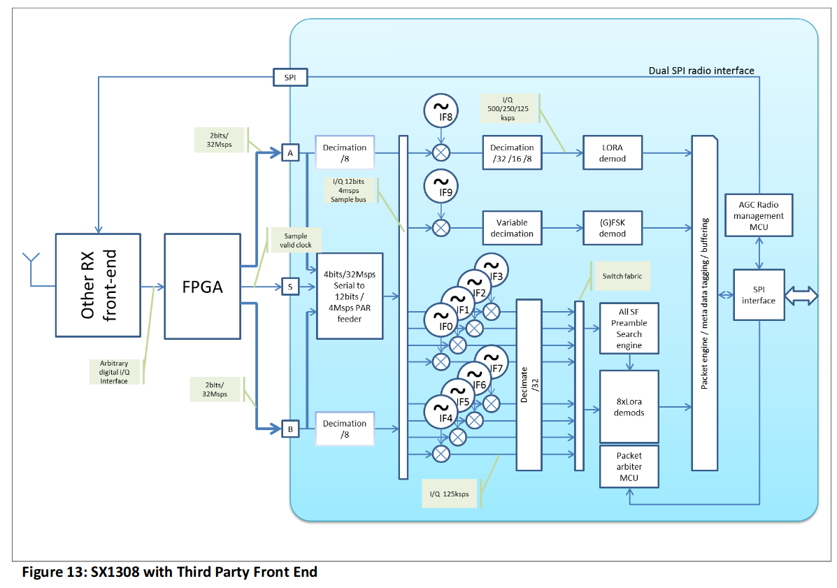
based on some old idea I’m trying to build a LoRa decoder. The idea is to decouple the radio interface (SX1257) from LoRa decoder (SX1301) to be able to supply samples also from other/multiple radio interfaces.
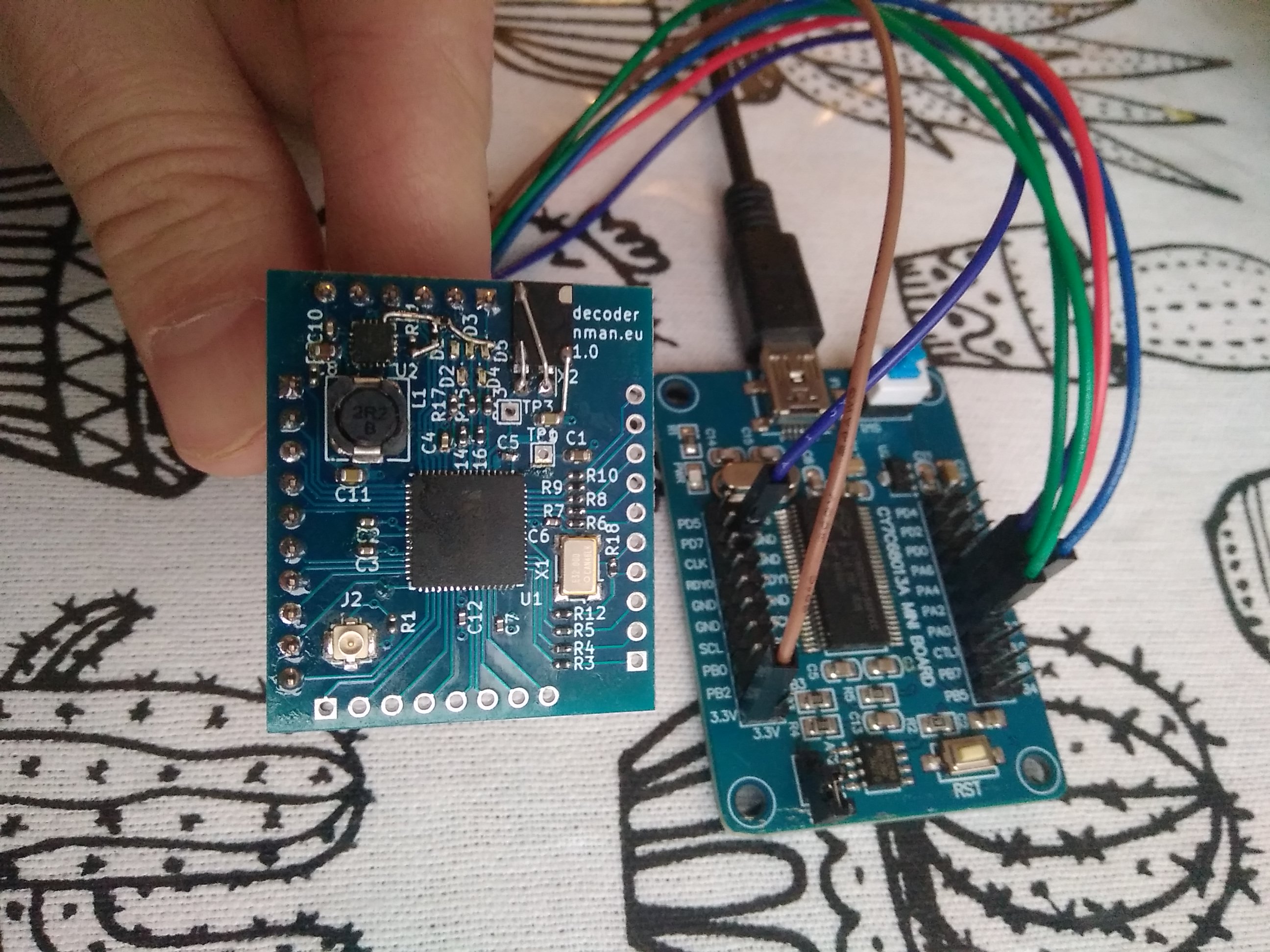
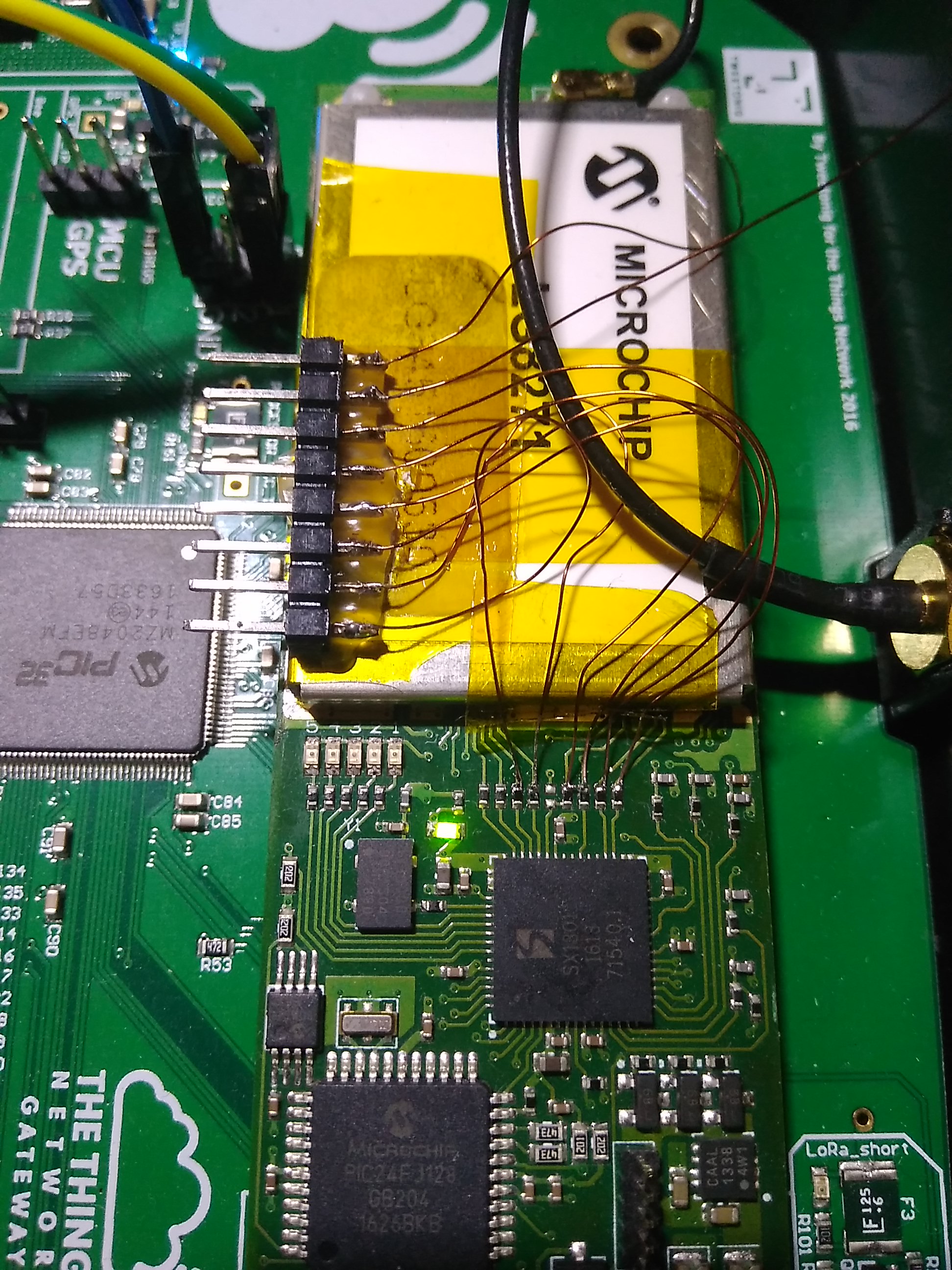
So far I was able to build a breakout board and connect it to PC using FX2LP:
I’ve written firmware for FX2LP to provide SPI comms and patched TTNs packet forwarder to communicate with my board. packet-forwarder.txt (3.9 KB)
Now I will need to understand the radio interface and I/Q sampling to provide it with some radio data thru FX2LPs high speed slave FIFO interface.
Is here someone who finds this project interesting and would like to help?
My current biggest question is how to configure the chip to accept data without trying to configure and control the radio, whether it is necessary to do the calibration and load AGC and arbitration firmware.
Is there someone who can provide some insight to these topics or dig something out of the source code because AFAIK official documentation doesn’t exist (not even for chip registers).
Interesting project. I don’t know enough about the specifics of the tech stack you are trying to create but I like the concept. With increased integration and the desire to add DSP functionality directly to the packet pipeline, there are opportunities to create these front-ends from scratch and place them directly into an FPGA so that you can build highly flexible SoC solutions.
To be clear here, my ultimate goal is to create lora decoder sw/hw module you can supply radio samples to (e.g. via HTTP + json) and it will reply with decoded packet and metadata. And a second part:
A cheap radio gateway module (e.g. rtl-sdr + rfm96 for downlink) which will communicate with decoder module to decode uplink msgs and submit them to TTN.
Decoder should be able to decode messages from multiple radio gw modules so anyone can try to use multichannel lora fairly cheap until he grows up to bigger scale.
I have one working TTNGW so my plan now is to capture IQ samples while transmitting a message from rfm95. Then I’ll try to supply these samples to my module and see if it can decode the message too.
Next step will be to add an FPGA to optimize the interface: 8/16bit on FX2LP to 4bit chA Q/I, chB Q/I.
I’ve tested FX2LP for capturing samples from the interface but it can only work up to 14MHz (14MB/s) but I need 32MHz or at least 16. I’ll keep trying with FT2232H.
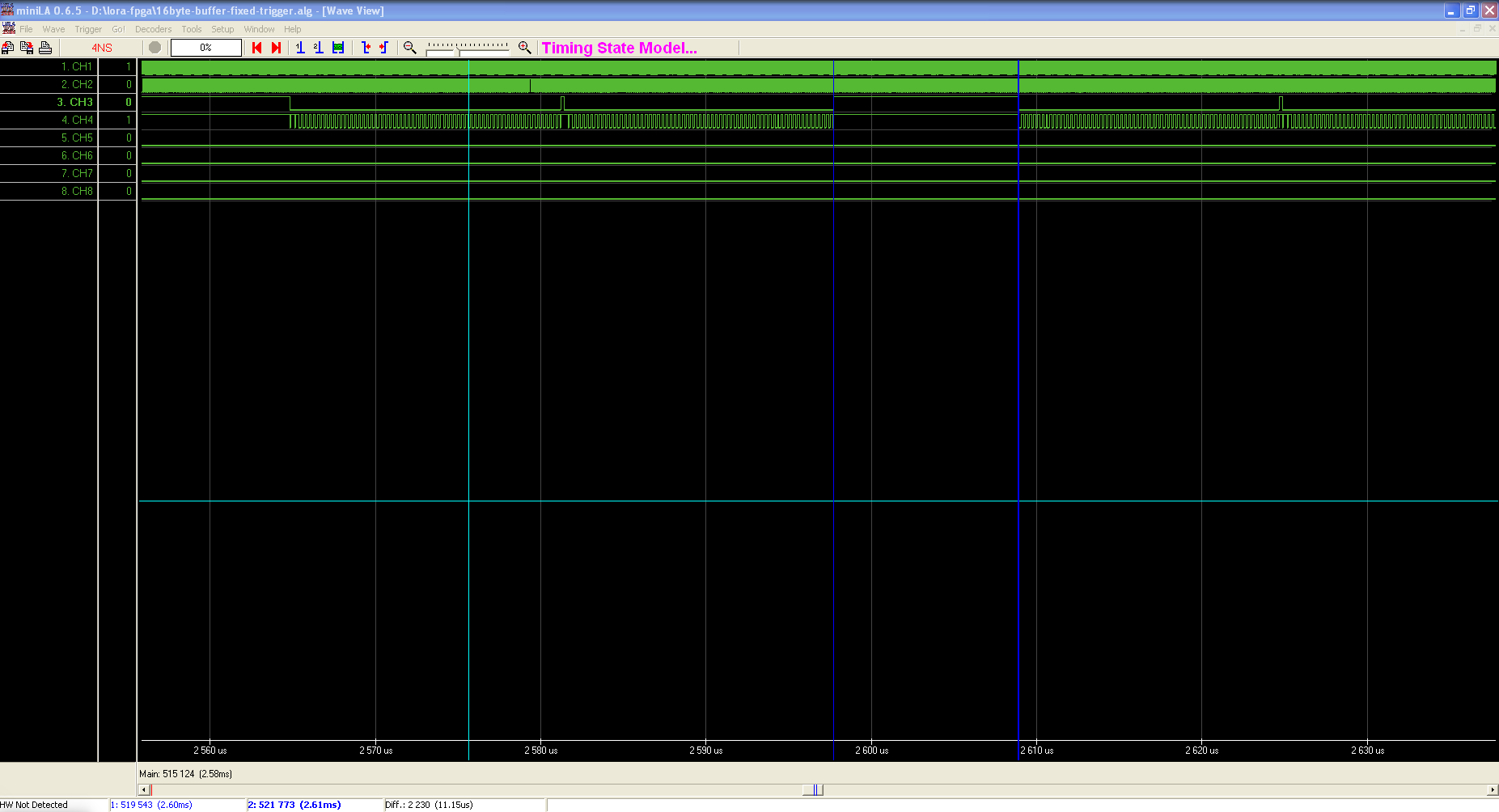
I started the FPGA design on MAX II but during testing it showed up that there are 13us windows of #TXE high signal on FT when it cannot accept data and the data needs to be buffered during this time.
CH1 - 60MHz from FT
CH2 - 32Mhz from LoRa radios
CH3 - #TXE from FT
CH4 - WR to FT
It means about 400 bytes of memory which MAX II doesn’t have so I needed to switch to a bigger FPGA: Spartan-6. Now finally I see roughly correct bitrates:
 59.01s total time  1693.311 MiB captured 31185.2 kB/s curr rate 29384.3 kB/s totalrate 0 dropouts
 60.01s total time  1723.778 MiB captured 31194.4 kB/s curr rate 29414.5 kB/s totalrate 0 dropouts
 61.01s total time  1754.232 MiB captured 31183.5 kB/s curr rate 29443.5 kB/s totalrate 0 dropouts
 62.01s total time  1784.691 MiB captured 31183.0 kB/s curr rate 29471.5 kB/s totalrate 0 dropouts
Next step is to write some decent sw for capturing the data and look at the data while transmitting a LoRaWAN packet.
I see your point but I have this board: https://www.aliexpress.com/item/1000006622145.html
Can you get spartan7 for under $20? The chip alone can be bought for under $5.
And as far as I can see, spartan6 is perfectly sufficient.
Today I fixed those error messages with firmware problems:
ERROR: Version of calibration firmware not expected, actual:145 expected:2
lgw_start:904: ERROR: Version of AGC firmware not expected, actual:145 expected:4
lgw_start:911: ERROR: Version of arbiter firmware not expected, actual:67 expected:1
Now it says:
   INFO Starting concentrator...                 DateTime=2020-01-09 02:10:04.847807398 +0100 CET m=+3.941202858
 lgw_connect:524: INFO: no FPGA detected or version not supported (v103)
 Note: success connecting the concentrator
 setup_sx125x:495: Note: SX125x #0 version register returned 0x00
 setup_sx125x:503: Note: SX125x #0 clock output disabled
 setup_sx125x:557: Note: SX125x #0 PLL start (attempt 1)
 setup_sx125x:557: Note: SX125x #0 PLL start (attempt 2)
 setup_sx125x:557: Note: SX125x #0 PLL start (attempt 3)
 setup_sx125x:557: Note: SX125x #0 PLL start (attempt 4)
 setup_sx125x:557: Note: SX125x #0 PLL start (attempt 5)
 ERROR: FAIL TO LOCK PLL
 setup_sx125x:495: Note: SX125x #1 version register returned 0x00
 setup_sx125x:500: Note: SX125x #1 clock output enabled
 setup_sx125x:557: Note: SX125x #1 PLL start (attempt 1)
setup_sx125x:557: Note: SX125x #1 PLL start (attempt 2)
setup_sx125x:557: Note: SX125x #1 PLL start (attempt 3)
setup_sx125x:557: Note: SX125x #1 PLL start (attempt 4)
setup_sx125x:557: Note: SX125x #1 PLL start (attempt 5)
ERROR: FAIL TO LOCK PLL
lgw_start:736: Note: calibration started (time: 2300 ms)
lgw_start:757: Note: calibration finished (status = 161)
WARNING: calibration could not access radio A
WARNING: calibration could not access radio B
WARNING: problem in calibration of radio A for image rejection
WARNING: problem in calibration of radio B for image rejection
Info: Initialising AGC firmware...
Info: putting back original RADIO_SELECT value
  INFO Concentrator started, packets can now be received and sent DateTime=2020-01-09 02:10:09.202137307 +0100 CET m=+8.295532662
Now it draws 260mA@3.3V and led blinks on start so it looks much more healthy. The problem was that I routed the 32MHz clock to a wrong pin (39 instead of 43).
I’m a bit stuck because of some troubles with clock input. Every time I try to share the onboard XO with both SX and FPGA, SX refuses to cooperate (firmware loading fails, low power consumption). I need to find a way how to correctly route the clock signal.
Currently my best option is to use 50MHz XO on FPGA board and PLL inside to convert to 32MHz and route the output to SX.
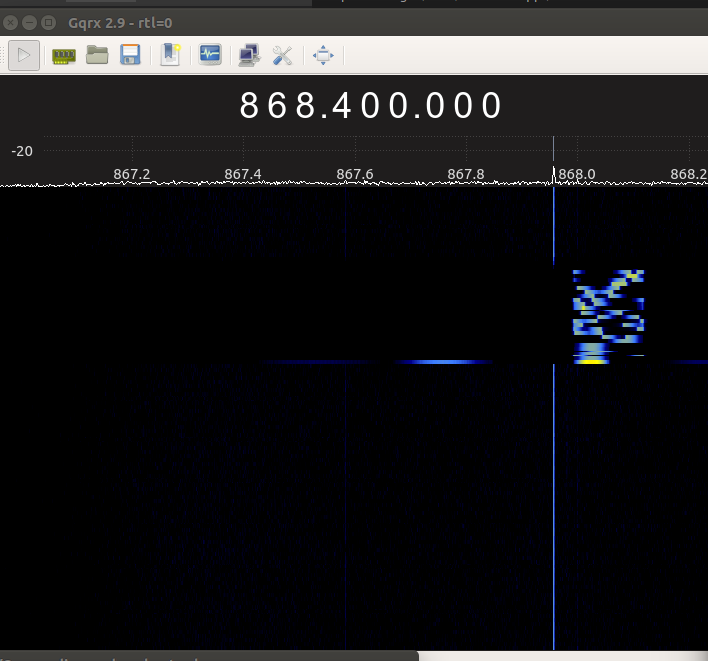
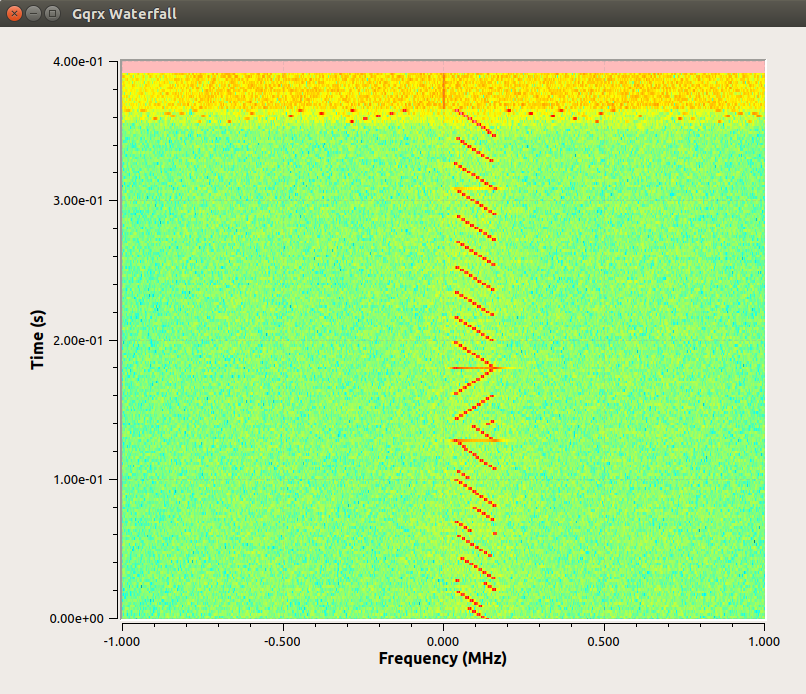
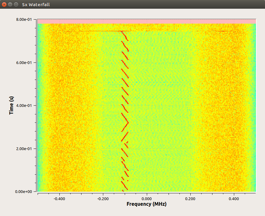
 I was able to decode the data. Here you can see lora packet from gqrx capture processed by GNU radio: