I am working on a concept where I use a chip antenna with a STM32WLE5. is it conceivable to use the same board layout as the generic node but minimise on components involved in the antenna circuit? for example could I
remove the RF and and analog switches
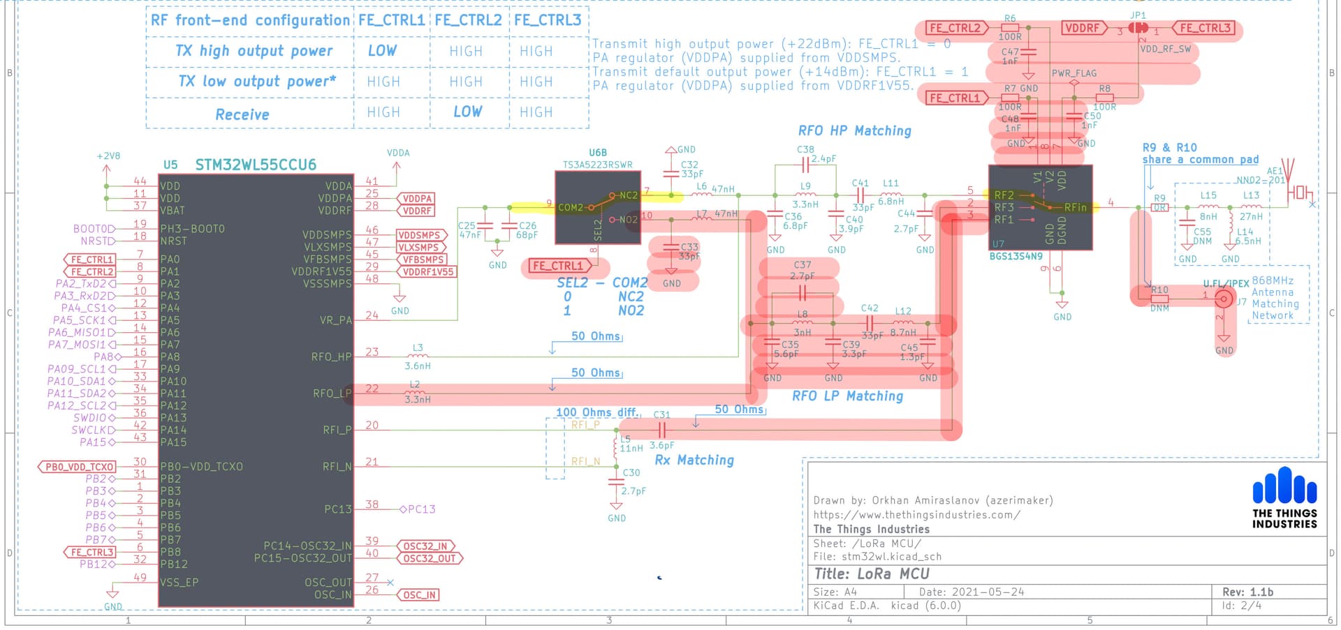
based on the schematics on GitHub, if I assume the switches are in the position shown remove the other circuits that would not be activated in the shown configuration.
This will result in a fixed power selection but the additional components add bulk to the BOM for my purposes in making the leanest node using a chip antenna.
I have marked components that I would remove in red highlighter.
I really hope you know what you are doing if you want to remove the low-pass filter and the antenna-switch for the receiver.
There are legal aspects you have to follow e.g. concerning emission of harmonics.
How do you receive MAC-commands from TTS without receiver-antenna? Or should it become a transmit-only node?
Thank you VERY much indeed for your reply. Let me describe what I am trying to make. We are helping people with Dementia remember (or be reminded really) to shut their doors though a series of sensors that detect door close/open, swing and ambient temperature. I have made a little LED Hub on ESP32 with a RFM69 and version with RM95- commonly available low power radio and Lora Transmitters) and want the device to work:
Point to point sending messages just to this hub
LoRaWAN/TTN - so that as we make more of these then we can pass info via a web interface to the head nurse.
I want to make 50 of these and need to keep the BOM cost down. I already have one functioning using an ATMEGA328p MCU with the above radios and get a sleep current of 4uA. However I need to switch out the MCU and the STM32WL works in all other respects. There are three problems:
Power - I want to use an CR2032 with minimum protection circuitary(buck/bost converter is lovely but expenive, hard to get hold of, and potential soldering nightmare) and achieve same if not better sleep current than 4uA. I know this is possible in spades with ST32WL but seems to come at the cost of additional components. The device only need to transmit and only receive once when it gets the downlink message at registration (for Lora version).
Antenna - I want to use a chip antenna like to the one of the Generic Node.
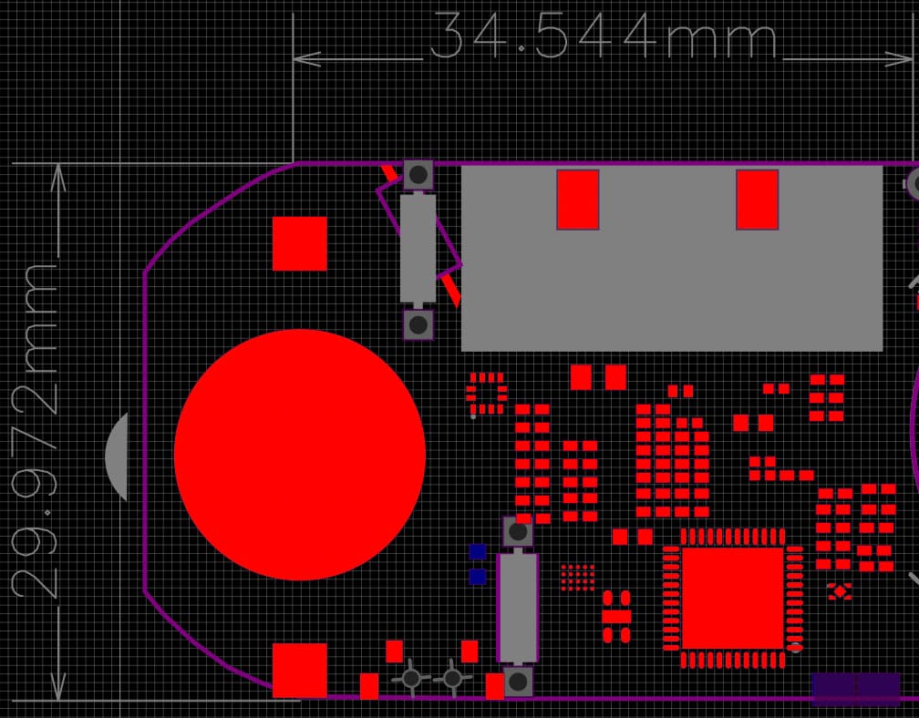
Board size - board must be 30mm x 35mm (space left for antenna marked in Grey is 23.5x10.5mm based on generic node)
So after minimising components, do I need to leave same space between the the STM32WL and start of board like in the Generic node - from top of MCU to start of antenna space is about 18mm, does this mean that I can’t design a chip an efficient antenna based design with my design constraints. Any help would be really appreciated.
As you can see from the image I only have 30cm - 18mm which leaves me only 12mm to place the MCU - so I am hoping that these space requirements are not a limitation and I can get help to find a way to have a more compact board.
I am looking at this reference design for a 2 layer board and if I can stick with 2 layers and achieve the above then that will mean that we can deploy to other care centres cheaply - somehow our solution is a combination of this design and the Generic node, looking for a way to the end of the rainbow! Thanks!
LoRaWAN nodes, and especially those on TTN, absolutely must receive in the receive windows, and they must act on the network management messages that are sent then.
Now I know! Many thanks that will help me further down. Sorry I guess I was just looking at the exchanges on the stack. So with that said what is the bare minimum needed with the above specs to drive an accelerometer, two reed switches, i2s sensor using tm32wl and chip antenna?
How will your device receive “only once” if it has no receiver circuitry? And as it’s not LoRaWAN without receive, it’s off topic for this forum.
That would be the one that relies on the PCB in important way, which even TTI staff didn’t design as they got the antenna design company to do it for them. And even then there is some debate about it’s effectiveness. Perhaps you should watch the presentation on the GNSE antenna from the designers themselves that were shown at the online mini-conference at the end of Jan.
Why so large? Or indeed, why MUST be that size.
Either you are hacking on the STM design or you are using the GNSE design. You can’t use both.
Trying to pluck at our heart strings so you can get a free design for something you are looking to sell to an industry that is not without some level of financial resource is just a little insulting.
How will they afford the gateway? And the subscription to the backend service that would need to be provided. If someone leaves the property and it transpires the alert didn’t get through because you were using the non-SLA TTN, will your insurers stand by you?
If a buck/boost circuit is a potential soldering nightmare, you’ll not cope well with the actual STM chip. If you are making batches of these, then you should really consider using a pick & place machine.
Or you could use a ready baked STM32WL based module with a standard chip antenna.
And if you use HF, you can’t get the current out the coin cells at Tx time and it’s debatable if you can for extended LF transmissions. I’m pretty sure there is a reason that Dragino dropped the coin cell idea for their door node and went with AAA. So with even a cursory search of devices would have come up with a ready made solution.
Is there a particular reason you want someone to look up the information in the data sheets we all have access to when you could do it yourself?
For instance, how many of the STM32WL chips support I2S?
What sort of package sizes do you see for accelerometers?
Reed switches can be mounted on PCBs but again, what sizes are good for door sensing when there can be a variable gap between it & the magnet as not all doors are flush or well fitted.
I’m going to have to assume I2S was a typo and I2C was intended. Even having shipped products using both, it’s a typo/speako I’ve made myself on occasion.
I2S is a streaming audio interface occasionally borrowed for other streaming data (low bandwidth radio IQ samples, or sensor readings with similar time domain behavior to audio).
I2C is a more generic interface to low/moderate bandwidth sensors and controllers of widely arbitrary purpose, of the sort you’d find in a LoRaWAN node project
I doubt there’s any STM32WL or EL that doesn’t support I2C, but it can also be bitbanged.
They do support I2C - I’ve a live GNSE (greenhouse), one on my desk, two Nucleo boards, a couple of RAK dev boards, several LoRa-E5’s plus tooling up to use the single core SOC.
But I’ll leave the sound monitoring potential to the OP.
I2S is actually a thing in care homes as you can use spikes in levels or even ML to detect things - like falling out of bed or shouting for help - no video required (that’s the important difference, video in old people’s bedrooms has been fully fleshed out as a big NO).
coin cell batteries have high internal impedance and can not source much current. It will struggle to transmit, particularly if you try and use the high power PA.
if it does manage to transmit without causing a brown-out, the battery capacity will suffer. Maybe thats not a problem in this use case
with a chip antenna and a small ground plane, antenna efficiency and range will be poor. Again, maybe OK in this use case, but just set your expectations correctly
(in fact the user’s arm becomes the antenna)
it would be a good idea to look inside a regular keyfob and see the style of antenna and the layout they use there
keep the schematic as close to the Semtech/STM ref design as possible. The more you change, the more you might regret it later
hey there!
I wanna jump in and recommend trying our latest technology, Antenna Intelligence Cloud (Online PCB Antenna Design Testing Tool | Ignion), which can give you an antenna design simulation for free (if it’s one antenna working in one frecuency band) in under 2h. That might help you giving the space and size constrictions you present. Again, this is a tool meant to help device designers, and it just takes a couple of minutes to submit. For a more complex report or service, you can always contact me, no problem!