A P-channel MOSFET turns on when it’s gate is negative relative to the source. So it turns ON ie lets the currants flow when it is at 0V. So as long as the source voltage is greater than Vgs, it will turn on when the gate is 0V.
P-Channel’s are used as high side switches so that a known voltage is presented to the load.
With VBatt=4.2V and VDD=3.3V Vgs will be -0.9V (when the MOSFET is closed) which is more than the listed -0.6V (Typical) Vgs which gives the impression the MOSFET will be open while it should stay closed with gate voltage of 3.3V.
I did have a sentence about WTF the R16 10K resistor was all about - if someone can link to the entire schematic plus tell me what GPIO7 is documented as being used for, I might be able to comment further.
The right hand side looks like a standard switch on VDD to an ADC, pulled to ground but again, without a schematic, it’s a bit hard to know why you’d want to know the VDD.
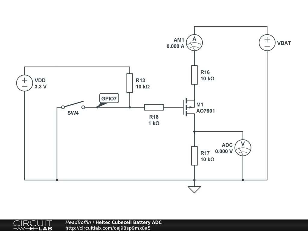
VBAT can be as high as 4.2V, R16 and R17 are a voltage divider so that only 1/2 VBAT is applied to the ADC input. Take gpio7 low to measure VBAT. Make it an input, so that it is pulled up to VDD, to disconnect the 20K path from VBAT to GND saving somewhere between 150 to 210 uA depending on the state of charge.
The gpio6 part of the circuit connects VDD to the VEXT pin on the CubeCell board. This can be used to power sensors (up to a limit which I can’t remember). Make gpio6 an input, before going to sleep so that the sensors are not powered. Take gpio6 low when you need to take sensor readings.
I suspect this battery measurement circuit is a potential cause of some of the reports of higher than expected sleep currents with Heltec dev boards.
A fully charged LiPo cell may create a high enough VGS to turn on the Mosfet and cause a 210 uA current to flow. The Mosfet will switch off when VBAT is sufficiently below VDD + VGS(th).
I am glad to hear that it is not so simple. Yesterday I did some research and found out that otherwise all circuits, to turn off the ADC voltage devider, consist of an N-channel and a P-channel mosfet. After seeing this circuit I thought Heltec might have done something clever here to save components. I had also sometimes measured 11ua deep sleep instead of my typical 3.2ua. I did not pay attention to the battery voltage. Perhaps it could also be caused by this.
This is the Schematic for HTCC-AB01. The one for HTCC-AB02 looks almost identical. Only the resistance values of R16 and R17 have been changed from 10k to 100k ohms.
But what board were you talking about then, the HTCC-AB01?
I did some measurements on my HTCC-AB01 almost 2 years ago and did not notice a higher than documented/expected deep sleep current of the board. I don’t remember the battery voltage of the LiPo used but for measurements I usually use fully charged batteries.
Often both are used to allow for the switching logic to be ‘normal’ where with just a P-channel mosfet the switching logic is inverted. (0 for on, 1 for off).
The advertised 3.5uA I was only able to measure when powering directly with 3.3V (not via battery connector).
When powering with Li-ion or LiPo cell via battery connector, the quiescent current of the voltage regulator will come into play and will (also) increase deep sleep current.
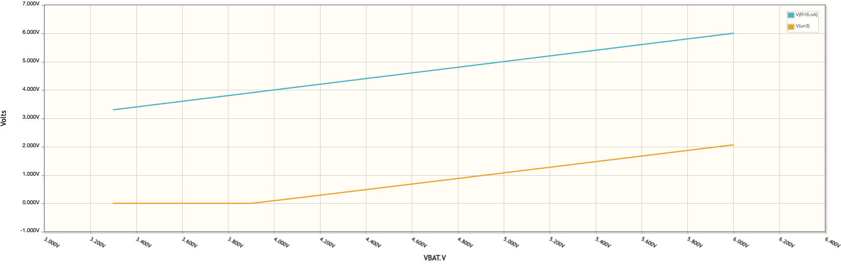
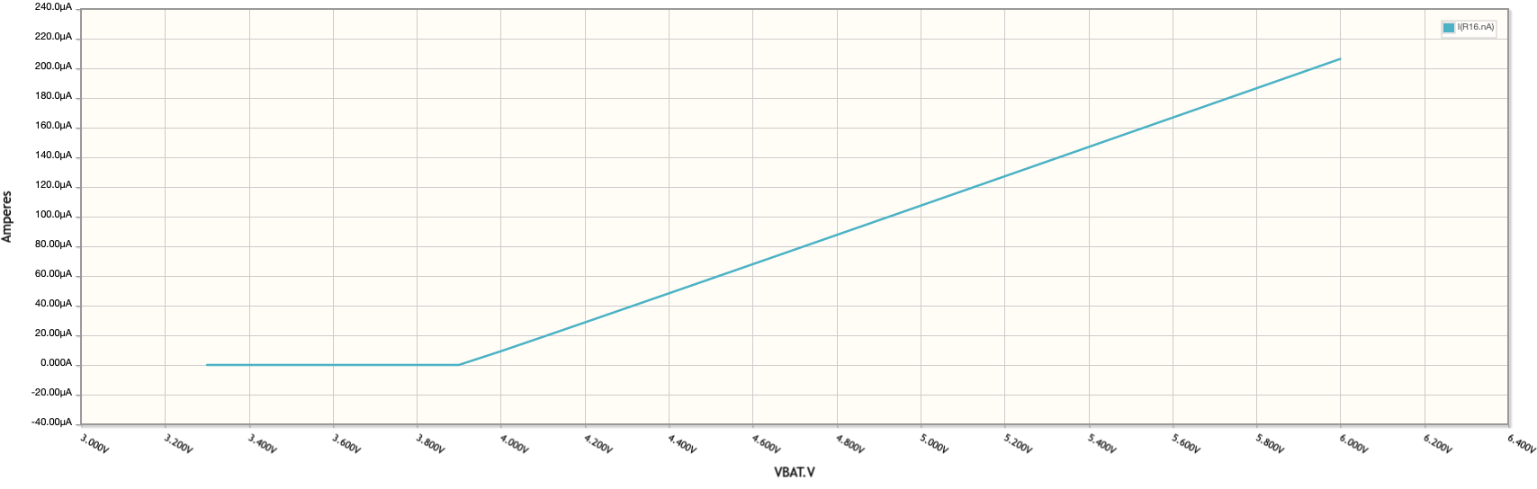
Having spotted the numbers/letters on the pins weren’t what I was seeing in my head, here’s a small simulation that actually confirms the original assumption, the LiPo will slowly discharge through the ADC divider until it reaches the difference between the 3.3 and the exact value that that half of the AO7801 is at (ie real world Vgs between -0.5 to -0.9V)
You can see the step at 3.9V, at 4.1V the drain is 19uA
The thinking behind this will be that LiPo’s tend to settle quite quickly to ~3.7V so it’s not losing too much energy, but still a bit of a waste.
I personally use BSS84’s after a disappointing incident with KiCAD. They have a Vgs of -1.6V so I’ve not really thought about the potential (pun intended) for loss of potential.
BSS84 is not identical to AO7801 and has different characteristics.
NXP BSS84 datasheet lists gate-source threshold voltage of Min -0.8V and Max -2V.
With VDD = 3.3V I would expect the kink in the graph to occur at 4.1V or higher instead of 3.9V. Based on the datasheet, for AO7801 I would expect it at 3.8V or higher.
Losing the will to live here - the schematic and my words say BSS84 but the graphs are set for the AO7801 with a Vgs of 0.6 - last I checked 3.3 + 0.6 = 3.9 but I’m beginning to doubt myself.
I’ve replaced the schematic.
Feel free to follow the CircuitLab link and try things out.
Does any one have an example of how to send AT commands when using the Ardunio mode. I see lots of things Around AT Enable / Disable but still no method to actually send a command. I just want to disable the Copyright message so I can use the UART.